1. 182mm silicon wafer vs. 210mm silicon wafer
Advantages of 210 silicon wafer:
① The increase in silicon wafer size can reduce costs and improve efficiency in many aspects of downstream processes. The cost reduction of large silicon wafers mainly comes from the cost reduction effects of "throughput" and "increased circumference of inconsistent areas".
Flux: As silicon wafers become larger, production capacity increases, and the corresponding equipment and manpower do not need to be increased, resulting in a cost reduction effect. In the battery segment, the output of the battery production line is calculated in units of silicon wafers. When the wafer area becomes larger, the production capacity of the battery cell also increases accordingly, which leads to dilution in labor, depreciation, and three fees. Compared with the M2 battery, the M12 battery can save 0.08 yuan/W and reduce 25.6%. The same is true for the component part. The increase in production capacity has led to the dilution of labor and depreciation.
Area increase: mainly at the component end and terminal power station. That is to say, when the size of wafers and modules increases, the amount of frames, solder strips, etc. also increases accordingly. However, the increase is less than the increase in size and area, which can save the cost per watt. This effect is mainly reflected in the baffles on the module side and the solder strips. This effect is mainly reflected in the frame and solder strips at the module end, as well as the brackets of the terminal power station.
②Whether it is N-type battery technology or perovskite stacking, the future will be based on 210.
Disadvantages of 210 silicon wafers (=disadvantages of 182 silicon wafers):
The existing production capacity cannot be upgraded from 156 to 210 through technological reform, and Perc batteries have been caught in a fierce price war. In such a market environment, battery manufacturers do not have enough motivation to add new battery production capacity. Therefore, in the short term, large-scale industrial application of 210 wafers cannot be realized temporarily. It is suitable for new factories to expand production and purchase new equipment to use 210 wafers.
Conclusion: One works hard in the present, the other focuses on the future.
It can be said that one of them is working hard in the present, and the other is looking to the future. They are neither good nor bad, but in the case of following the trend of history, they will be absorbed by the times. In the future, with the widespread use of large silicon wafers, it is expected thatPhotovoltaic IndustryA new round of innovation will come.
2. Semiconductor silicon wafers VS photovoltaic silicon wafers
Both are made of single crystal silicon.
Photovoltaic silicon wafer
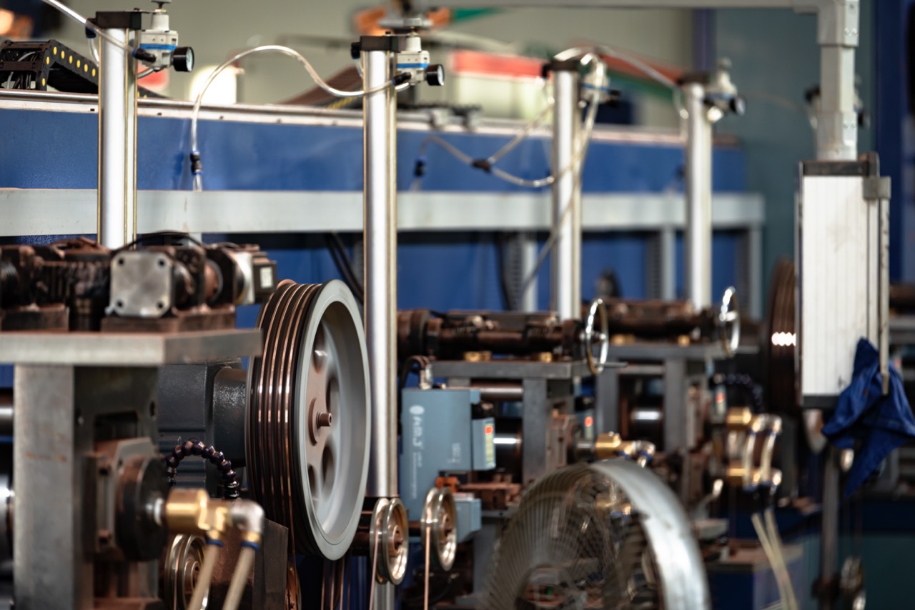
The requirements for parameters such as purity and warpage are low, and the manufacturing process is relatively simple.
Take monocrystalline silicon cells as an example:
The first step is cutting and squaring. First, the single crystal silicon rod is cut into square rods according to the size requirements, and then the four corners of the square rod are rounded.
The second step is pickling, which is mainly to remove impurities on the surface of the single crystal square rod.
The third step is slicing, first stick the cleaned square sticks on the work board. Then put the work board on the slicer and cut it according to the set process parameters.
Finally, the single crystal silicon wafers are cleaned and monitored for surface smoothness, resistivity, and other parameters.
Semiconductor silicon wafer
Semiconductor silicon wafers have higher requirements than photovoltaic silicon wafers. First of all, all silicon wafers used in the semiconductor industry are single crystal silicon. The purpose is to ensure that the electrical characteristics of each bit of silicon wafer are the same. In terms of shape and size, single crystal silicon wafers used for photovoltaics are square. They are mainly available in products with side lengths of 125 mm, 150 mm and 156 mm. Single crystal silicon wafers for semiconductors are round, with wafer diameters of 150 mm (6-inch wafers), 200 mm (8-inch wafers) and 300 mm (12-inch wafers).
In terms of purity, the purity of monocrystalline silicon wafers used for photovoltaics requires a silicon content between 4N and 6N (99.99%-99.9999%). However, monocrystalline silicon wafers used for semiconductors are about 9N (99.9999999%) to 11N (99.9999999%), and the minimum purity required is 1,000 times that of photovoltaic monocrystalline silicon wafers. Therefore, the purity of semiconductor wafers is much higher than that of photovoltaic wafers.
From the appearance point of view, the surface flatness, smoothness and cleanliness of semiconductor silicon wafers are higher than those of photovoltaic silicon wafers. Purity is the biggest difference between photovoltaic single crystal silicon wafers and semiconductor single crystal silicon wafers.
3. P-type battery VS N-type battery
The future belongs to N-type battery world
Advantages of N-type batteries over P-type batteries.
(1) High conversion efficiency. At present, the average mass production efficiency of PERC superimposed with SE technology is: P-type cells are 22%-22.4%, TOPCon is 22.4%-23.1%, and HJT in N-type cells is 23%-23.6%.
(2) High bifaciality. The bifaciality of P-type PERC cells is about 75%, while that of N-TOPCon exceeds 85%, and that of N-HJT exceeds 95%.
(3) Low temperature coefficient. The temperature coefficient of N-type batteries is lower than that of P-type batteries, making them suitable for applications in higher temperature scenarios, such as Africa, the Middle East, and other regions with good radiation conditions.